Basic Logic Gates
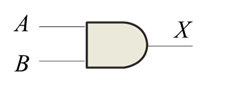
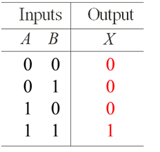
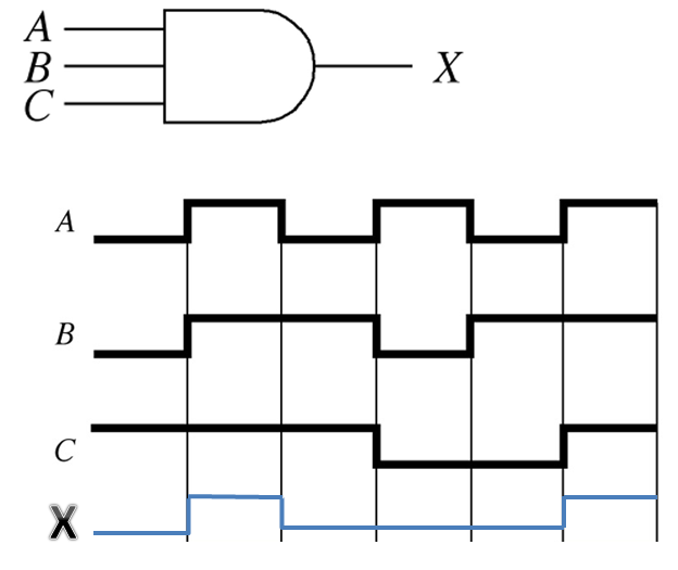
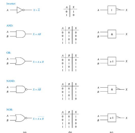
The output of an AND gate is true (logic 1) if and only if all of the inputs to the gate are true (logic 1). A truth table is used to illustrate how the output of a gate responds to all possible combinations on the inputs to the gate. The AND gate can be illustrated with a series connection of manual switches or transistor switches.
The AND operation is usually shown with a dot between the variables but it may be implied (no dot). Thus, the AND operation is written as X = A .B or X = AB.
The number of combinations of a truth table is equal to 2N where N is the number of inputs. So a 2 input gate would have 22 outputs or 4.
Example waveform:
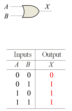
The output of an OR gate is true (logic 1) if any or all of the inputs are true (logic 1). The OR gate can be illustrated with a parallel connection of manual switches or transistor switches.
The Boolean Expression for a two input OR gate is X = A + B. The OR operation is shown with a plus sign (+) between the variables. Thus, the OR operation is written as X = A + B.
The only time the output of an OR gate is low is when all the inputs are low.
Example waveform:
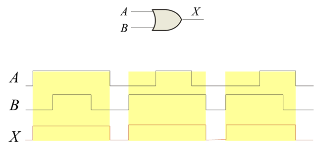
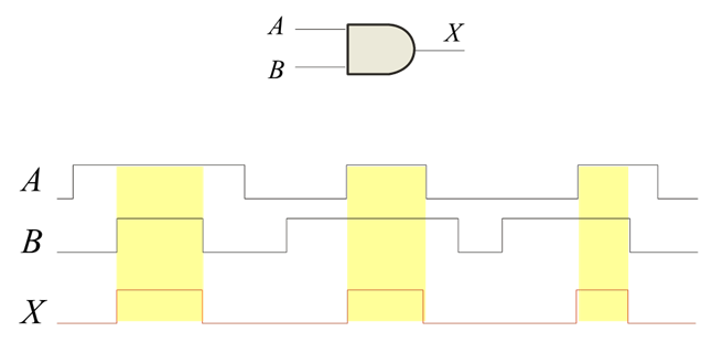
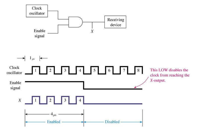
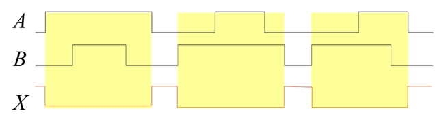
A timing diagram is a graph of the output of a logic gate with respect to the inputs of the gate. A timing diagram plots voltage (vertical) with respect to time (horizontal). A timing can also be seen as waveforms on an oscilloscope or on a logic analyzer. In order to determine the proper output waveform from a logic gate, simply divide the input diagrams into time segments where the inputs are constant and determine the state of the output (high or low) for that segment from the truth table. If the situation comes up where it does not make any difference which state an input is in (either way the output does not change), the input is said to be in a don't care condition.
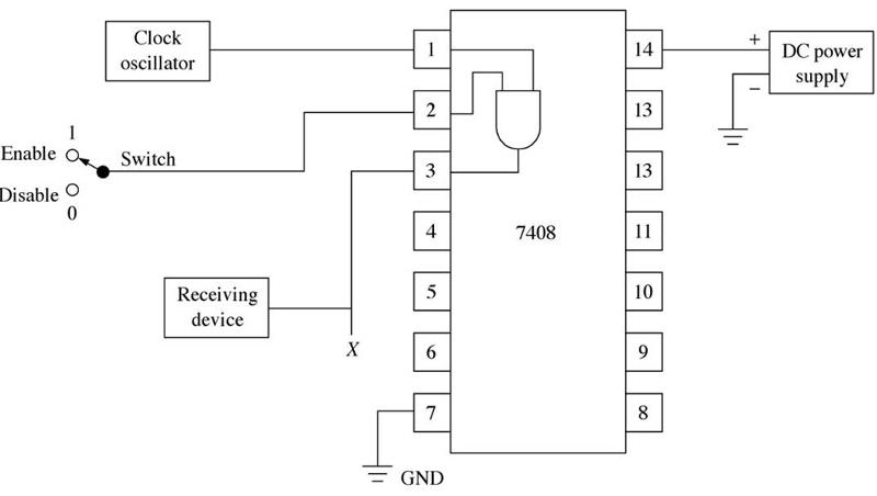
Troubleshooting is the steps used to locate the fault or trouble in a circuit. The first step in troubleshooting is to understand how a particular IC is supposed to work. One tool for digital troubleshooting is the logic probe. The logic probe is used to indicate the High (1), Low (0), or floating (open circuit) condition of any pin on a digital IC. The second tool used in digital troubleshooting is the logic pulser. The pulser is used to inject a series of High and Low pulse signals into a logic gate. To test an AND gate, connect all inputs but one high. Connect the remaining input to the pulser and check the output with the probe. The output should be pulsing. To test an OR gate, connect all inputs except one low. Connect the unused input to the pulser and check the output with the probe. The output should again be pulsing. An experienced technician can use visual inspection as a troubleshooting tool. The technician will look for conditions such as a misaligned or broken IC pins, cracked circuit board, solder bridges and burnt or overheated components.
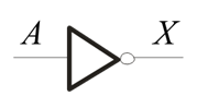
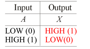
The output of an inverter is the complement (opposite) of the input. When the input to an inverter is high (1) the output is low (0); and when the input is low, the output is high. In Boolean Algebra the inverter operation is shown by placing a bar over the variable.
![]()
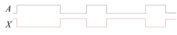
The waveform on the output of an inverter would look like the exact opposite of the waveform on the input. The inverter is also often called a NOT gate.
Example waveforms:
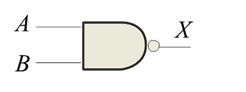
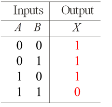
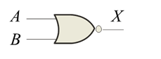
The NAND gate is the same function as an AND gate with the output inverted. The logic symbol for a NAND gate is the same as an AND gate except it has a small bubble on the output to indicate that the output is inverted.
The NAND operation is shown with a dot between the variables and an overbar covering them. Thus, the NAND operation is written as X = ![]() (Alternatively, X =
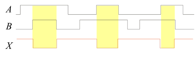
(Alternatively, X =![]() ). The truth table for the NAND gate shows the output to be just the inverse of the output of an AND gate. The only time the output is low is when all the inputs are high.) The output of a NAND gate can be shown with a timing diagram in the same manner that the output of the AND and OR gate were developed.
). The truth table for the NAND gate shows the output to be just the inverse of the output of an AND gate. The only time the output is low is when all the inputs are high.) The output of a NAND gate can be shown with a timing diagram in the same manner that the output of the AND and OR gate were developed.
Example Waveform:
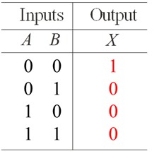
The NOR gate is the same as an OR gate with the output inverted. The NOR gate logic symbol is an OR gate with a bubble on the output to indicate an inverted output. The NOR operation is shown with a plus sign (+) between the variables and an overbar covering them. Thus, the NOR operation is written as X = ![]() .
.
The NOR gate truth table is the OR gate truth table with the output inverted. (The only time the output is high is when all the inputs are low.) The output of a NOR gate can be demonstrated with a timing diagram. The output is developed one segment at a time as the inputs change. The output again will follow the truth table.
Example Waveform:

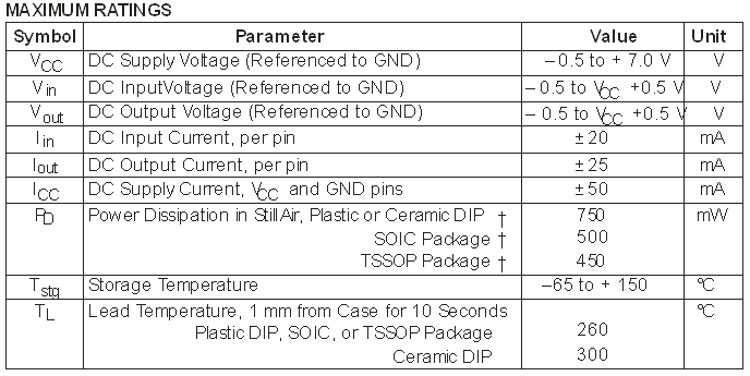
Data sheets include limits and conditions set by the manufacturer as well as DC and AC characteristics. For example, some maximum ratings for a 74HC00A are:
The AND gate and the OR gate are basic building blocks that will be used to construct more complex logic functions. the OR gate is sometimes called the "Either/Or Both" gate and the AND gate is sometimes called the "Coincidence" gate. These two gates, when combined with the NOT gate, can be used to construct about any logic function desirable.
The output waveform can most easily be determined if the input signals are first broken up into time segments where in each time segment the inputs are constant. Whenever an input changes, mark another time segment. Then, for each time segment determine the state of the output from the truth table for that logic gage. If this is repeated for each time segment then the result should be a continuous waveform on the output.
The NAND and the NOR logic gates are sometimes called the universal logic gates because the three basic building blocks of all logic (AND, OR and Inverter) can be accomplished using only NAND gates or using only NOR gates. All complex logic functions can be achieved using AND, OR and Inverter gates. If NAND and NOR gates are universal, then all complex functions can be accomplished using only NAND gates or using only NOR gates. This makes the NAND gate and the NOR gate very powerful gates. For this reason, many logic families will use a large number of NAND gates or a large number of NOR gates. The TTL logic family, for example, has a large number of the available circuits that are NAND logic gates.
Several of the basic logic gates are used to form a more complex function with combinational logic. A Boolean equation can be used to describe any combinational logic circuit. The Boolean equation is written in a form that will satisfy the problem.
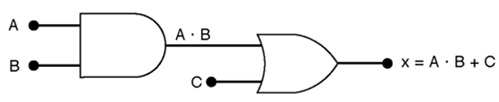
We have seen how to express single gate expressions like X=A+B for an OR gate and F=D*G for the AND gate. Now we will look at combinational logic and Boolean expressions.
Converting a logic diagram to a Boolean expression
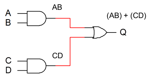
Given the logic gates below. First look at how the gates are connected to each other. Notice how there are 2 sets of AND gates going into an OR gate. Lay it out logically like this (something AND something) OR (something AND something).
In this case it would be: (A AND B) OR (C AND B) Change the AND / OR to their Boolean symbols and you have: (A*B) + (C*D). So Q=(AB) + (CD) (Notice The AND gates are generally grouped together with parenthesis. I also dropped the *. When terms are placed next to one another a multiplication is implied.
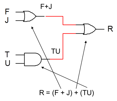
Here is another example
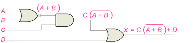
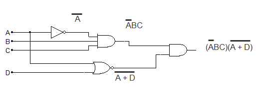
When NAND and NOR gates are used. Just make sure you place the bar over the expression that is inverted.
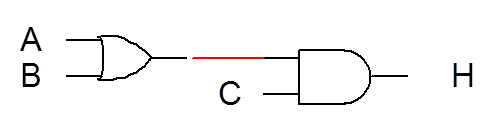
Take the expression: H=(A+B)C
This tells us that A is ORed with B and that is ANDed with C. The logic gates would look like this.
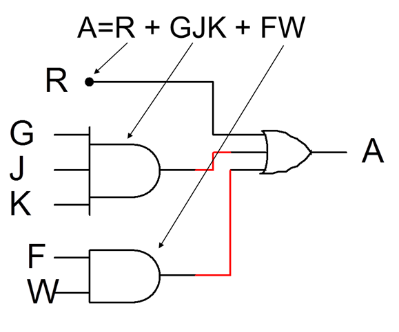
How about: A = R + GJK + FW
More examples:
Is it A•B ORed with C? Is it A ANDed with B+C?
Order of precedence for Boolean algebra: AND before OR.
The following is correct.
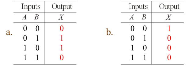
Use the following truthtables to answer the questions.
Truth Tables: