Shift Registers
Shift Register Basics
- A register acts as a temporary storage device for a group of data bits.
- A shift register is used to move data to the left or to the right by one bit for each input clock pulse.
- Parallel load means to load all flip-flops of a register at one time.
- Serial load means to load the flip-flop of a register one bit at a time.
- The number of clock pulses required to shift all bits of a register completely in or completely out of the register is equal to the number of flip-flops in the register.
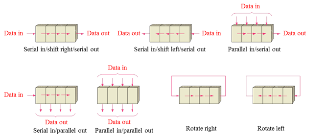
- There are four basic register configurations:
- Parallel-in, Parallel-out.
- Serial-in, Serial-out (both left shift and right shift).
- Parallel-in, Serial-out (right shift).
- Serial-in, Parallel-out (right shift).

- Many computers operate on parallel data; but, this data must be converted to serial format to be sent over phone lines.
- ICs called UARTs are used to interface microprocessors and parallel data to communications links that use serial data.
- This parallel-to-serial conversion and serial-to-parallel conversion can be performed by shift registers.
- Shift registers are available in IC form or can be constructed from discrete flip-flops as is shown here with a five-bit serial-in serial-out register.
- Each clock pulse will move an input bit to the next flip-flop. For example, a 1 is shown as it moves across.

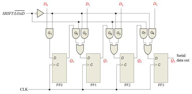
Parallel-to-Serial Conversion
- In order to construct a right shift register, the outputs of each flop-flop (Q and
 ) must be connected to the inputs (J and K or D) of the flip-flop to its right.
- A shift register must also have all clock inputs ties to a common clock signal so they will all change state at the same time.
- The asynchronous inputs (set and reset) for each flip-flop can be used to provide the parallel load.
- The output of a right shift register will appear at the Q output of the LSB. The LSB will appear first at the output.
- The output of a left shift register will appear at the Q output of the MSB. The MSB will appear first at the output.
Recirculating Register
- By taking the serial output (Q and
 of the LSB) and connecting it back to the serial input (J and K of the MSB) a recirculating register can be constructed.
- In the recirculating register, the original data will not be lost.
Serial-to-Parallel Conversion
- Parallel data can be taken from a register by reading the Q output of each flip-flop.
- Serial data can be applied to a shift register by applying one bit at a time to the MSB input for a shift right register.
- For a shift left register, data must be entered one bit at a time at the LSB.
- A strobe line is used to enable the clock so that the register is shifted only once for each data bit.

Ring Shift Counter and Johnson Shift Counter
- Ring shift counters and Johnson shift counters are used to generate sequential control waveforms.
- The Ring shift counter is a recirculating register in which the serial output is connected back to the serial input.
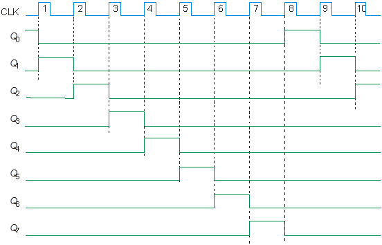
- The Q outputs of the Ring shift counter will go high for one clock pulse one at a time in sequence.
- The Ring shift counter must be initially set-up with a single flip-flop set and all others reset.
- The initial condition of the Ring shift counter will be shifted through the register on each clock pulse.
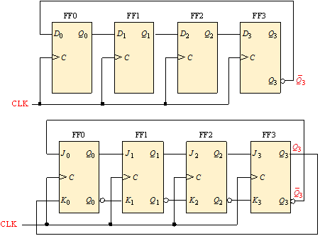
- The Ring counter can be made with either D-type or J-K Flip-Flops.


- The Johnson shift counter has the recirculating lines crossed such that the inverse of the output data is fed back to the input.
- Each Q output of the Johnson shift counter is a square wave (50% duty cycle).
- Each Q output of the Johnson shift counter is offset or shifted by one clock pulse.
- The Johnson shift counter must be initially reset (all flip-flops zero).
- The Johnson counter is also called a Twisted Ring counter.


Shift Register ICs
- The 74164 is an 8-bit serial-in, parallel-out shift register.
- The 74164 has two data input, one of which can be used as a high active enable.
- The 74164 also has a master reset for all flip-flops.

Sample waveforms for the 74HC164A are shown. Notice that B acts as an active HIGH enable for the data on A.

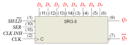
- The 74165 is an 8-bit serial or parallel-in, serial-out shift register
- The 74165 has a low active parallel-load terminal (XXX).
- The 74165 also has a chip enable (XXX) for hold of data or enabling the shift. The chip-enable can also be used as a strobe input for serial loading of data.

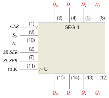
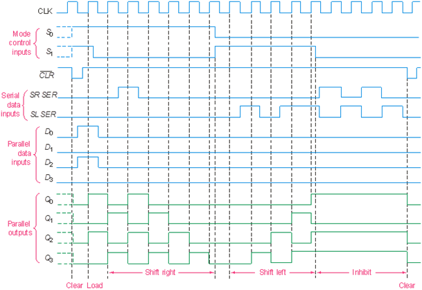
- The 74194 is a 4-bit bidirectional universal shift register.
- The 74194 is capable of shift-left, shift-right, parallel-in, parallel-out, serial-in, or serial-out.
- The 74194 has two mode control inputs (S0 and S1) which are used to select the desired operating mode.
- A three-state output can be HIGH, LOW or a float.
- When the three-state circuit is enabled, the output is the same as the input. When the circuit is disabled, the output is "high-impedance" or floating.
- The three-state buffers are used when connecting the output of more than one register together to a single input.
- The 74194 is considered a universal shift register which has both serial and parallel input and output capability.


System Design Applications for Shift Registers
-
A Ring shift counter can be used to generate accurately timed sequence pulses.
- A Johnson ring counter can be used to generate pulses of different lengths and occurring at different times.
- Shift registers can be used to convert serial data to parallel data or to convert parallel data to a serial bit string.
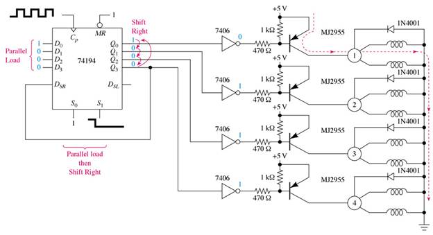
Driving a Stepper Motor with a Shift Register
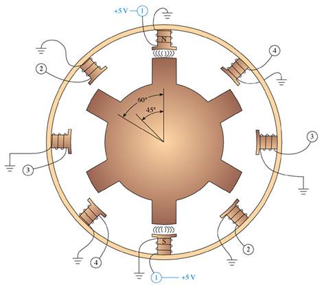
- Stepper motors make their rotation in discreet steps. This stepping action is caused by digital levels on the motor inputs.
- Shift registers make excellent stepper motor drivers.
- The 74194 is a 4-bit register that can be parallel loaded with the correct binary pattern and then shifted left or right to determine the direction of rotation.
- The clock frequency of the shift register will determine the speed of the motor's rotation.


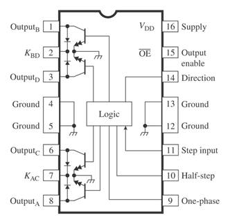
Stepper motor driver ICs
UCN5804B
Drives four phase unipolar stepper motors
May use one-phase, two phase, and half step

Three-State Buffers, Latches, and Transceivers
- A group of flip-flops is called a register and function as a buffer, a latch or a transceiver.
- The three-state buffer can be used to interface several device outputs to one set of inputs.
- A buffer will pass a digital bit from it input to its output unchanged when the buffer is enabled.
- The 74LS244 is an octal (8) three-state buffer.
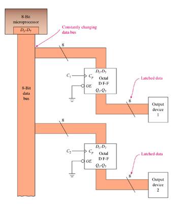
- A latch is a flip-flop that can be used to remember digital data.
- An 8-bit latch can be used to interface the output of a microprocessor to other devices.
- The 74LS373 octal latch and the 74LS374 octal D flip-flop are popular microprocessor interface chips.

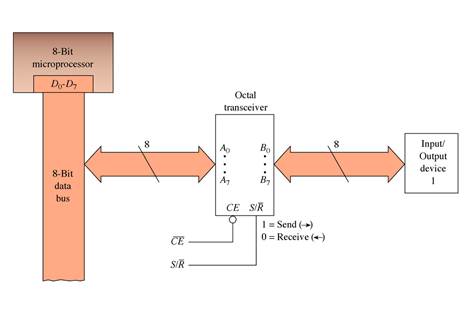
- A transceiver is a bidirectional buffer.
- With a transceiver, a microprocessor can receive data from an I/O device or can send data out to an I/O device over the same set of common lines (data bus).
- The 74LS245 octal 3-state transceiver uses two 3-state buffers for each set of data lines.

Additional Notes
An important application of the shift register is a delay circuit for a bit string. The time that the but takes to propagate through the shift register is a function of both the clock frequency and the number of flip-flops in the register. If a clock signal of 10 usec is used to clock an 8-bit shift register than it will take a total of 80 usec (8 × 10 usec) for a bit at the input of the register to appear on the output. In addition, the shift register can be tapped at each ! output as a function of multiples of the clock frequency. The first Q output will be delayed by 10 usec, the second by 20 usec, the third by 30 usec, and etc. A series of data bits applied to the input of a shift register can then be delayed in the shift register by multiples of the clock frequency.
